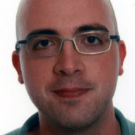
Jordi Arbiol
Born in Molins de Rei (Catalonia), 1975. Received his BSc in Physics at Universitat de Barcelona (UB) in 1997, where he also obtained his PhD (European Doctorate and PhD Extraordinary Award) in 2001 in the field of transmission electron microscopy (TEM) applied to nanostructured materials.

He also worked at the microscopy facilities and as Assistant Professor at University of Barcelona (UB), focusing in TEM advanced techniques, such as HAADF electron tomography, HREELS and in general high resolution (S)TEM. From 2009 to 2015 he was group leader and Scientific Supervisor of the electron microscopy facilities at Institut de Ciència de Materials de Barcelona, ICMAB-CSIC.
He is currently the leader of the Group of Advanced Electron Nanoscopy at ICN2. Since 2013 he is Vice-President of the Spanish Microscopy Society (SME), and since 2009 he was Member of its Executive Board.
The aim of Prof. Arbiol’s group is developing and applying Electron Nanometrology tools such as Transmission Electron Microscopy advanced techniques and related spectroscopies (EELS, EDX and CL) to study the structural and chemical properties of non-planar nanostructures (e.g.: nanowires). In addition the group has an excellent expertise in performing direct correlation between the structural and chemical properties at the atomic scale and the physical properties at sub-nanometer scale (photonics, plasmonics and phononics).
In 2015 he has received the 2014 EMS (European Microscopy Society) Outstanding Paper Award. In 2014 he was awarded with the EU40 Materials Prize (E-MRS) and was listed in the 2014 Top 40 under 40 Power List by The Analytical Scientist. He is author or co-author of more than 235 publications in peer-reviewed international journals (H = 46 WoS), 1 Book, 1 Book as Editor and 5 book chapters. He has presented 2 Plenary Lectures, 2 Keynote and 27 Invited talks in the last 5 years at International Conferences and 25 Invited Seminars Worldwide.
Research Interests
The increasing interest in Materials Science, Nanoscience and Nanotechnology has created a serious global need for the development of nanoscopy tools in order to be able to observe and chemically analyze the synthesized nanostructures at atomic scale. Exploring the limits of physical resolution in advanced electron microscopy and understanding the ultimate behavior of materials at the nanoscale and their related properties are the central aims of my research.
The newest research lines we are working in are based on single atom recognition and localization in embedded quantum structures. In parallel I am interested in finding methodologies to perform a direct correlation between the structural and chemical properties at the atomic scale and the physical properties at sub-nanometer scale (photonics, plasmonics and phononics).
This site uses cookies.
Some of these cookies are essential, while others help us improve your experience by providing insights into how the site is being used.
For more detailed information on the cookies we use, please check our Privacy Policy.
-
Necessary cookies enable core functionality. The website cannot function properly without these cookies, and can only be disabled by changing your browser preferences.